In this rapidly evolving world of technology, the demand for more powerful and efficient electronic devices continues to rise. This is where patterned silicon wafers come into play. They are actually making a huge mark in the market.

These wafers are a crucial component in the manufacturing of advanced electronic devices, making them essential for the future of technology. But what exactly are patterned silicon wafers, and why are they so important? Let’s find out!
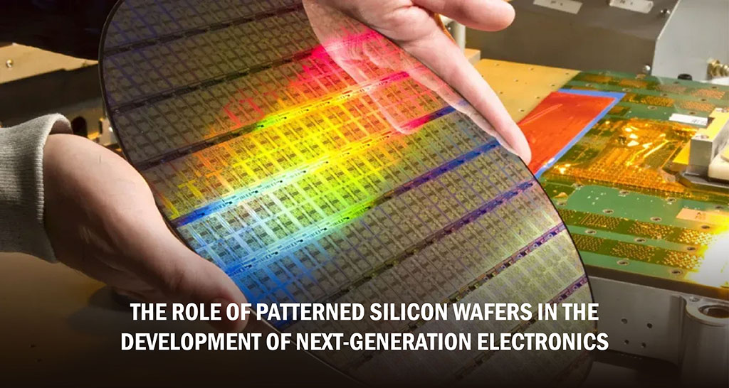
What Are Patterned Silicon Wafers?
Patterned silicon wafers are thin slices of silicon that have been etched with a specific pattern. This pattern is created through a process called photolithography, which involves using light to transfer a pattern onto the wafer’s surface. This pattern is essential for creating the intricate circuits found in modern electronic devices.
The process of making patterned wafers starts with a plain silicon wafer. A photosensitive material is applied to the wafer, and ultraviolet light is used to create a chemical reaction that forms the desired pattern. This pattern is then etched into the wafer, creating the tiny circuits needed for electronic devices.
Importance of Reliable Suppliers
When sourcing patterned silicon wafers, it’s crucial to connect with reliable suppliers. High-quality wafers are essential for achieving the desired performance and reliability in your electronic devices. Working with a trusted supplier ensures that you receive wafers that meet stringent quality standards. Quality suppliers can provide you with several benefits.
Consistent Quality: You can expect uniform and defect-free wafers that perform reliably in your applications.
Technical Support: Good suppliers offer technical support to help you with any issues or questions related to the wafers.
Timely Delivery: Reliable suppliers ensure that you receive your wafers on time, helping you maintain your production schedule.
When looking for patterned silicon wafers, consider suppliers who have a proven track record of delivering high-quality products. These wafers are crucial for achieving the performance and quality needed in modern electronics. Ensuring you have high-quality wafers can make a significant difference in your products and overall success in the technology industry.
Applications of Patterned Silicon Wafers
Microelectronics
Patterned wafers are widely used in microelectronics. They are essential for creating integrated circuits, microprocessors, and other small electronic components. These components are found in everything from smartphones to computers, making patterned silicon wafers a cornerstone of modern technology.
Medical Devices
In the medical field, silicon wafers are used to create small, precise devices such as hearing aids and pacemakers. These devices require exact control over electrical signals, which patterned silicon wafers provide. Additionally, biomedical sensors and nanotechnology used in medicine also rely on these advanced wafers.
Automotive Technology
The automotive industry is increasingly adding advanced electronics to vehicles. Patterned silicon wafers are used to create the sophisticated chipsets and sensors found in modern cars. These include driver assistance systems, navigation systems, and even the emerging technology of autonomous vehicles.
The Importance and Advantages of Patterned Silicon Wafers
Enhancing Device Performance
Patterned silicon wafers play a critical role in improving the performance of electronic devices. The precise etching process creates tiny channels that improve heat dissipation, leading to better overall device performance. This allows manufacturers to create smaller and more powerful devices, which is crucial in today’s push for more compact and high-performing electronics.
Cost-Effectiveness
One significant benefit of using patterned silicon wafers is their cost-effectiveness. The photolithography process used to create these wafers is efficient and reduces the need for additional materials and steps, making the production of electronic components more affordable.
Reliability and Consistency
Patterned silicon wafers offer a high degree of reliability and consistency. The precise patterns ensure that each wafer performs exactly as intended, which is essential for manufacturing complex electronic components. This consistency helps reduce defects and improve the overall quality of the final product.
Dependability
These wafers provide a high degree of uniformity, making them dependable for various applications. This uniformity is crucial for quality assurance testing and ensures that devices function as expected.
Flexibility in Design
Engineers have greater flexibility when designing new devices with patterned silicon wafers. Adjusting parameters such as line widths and spacing allows for easier experimentation and optimization, which is crucial for developing new and innovative electronic products.
The Future of Patterned Silicon Wafers
Emerging Trends
The field of patterned silicon wafers continues to evolve with new techniques and technologies. Innovations like block copolymer (BCP) lithography and directed self-assembly (DSA) are pushing the boundaries of what can be achieved with these wafers. These advancements are expected to lead to even more efficient and powerful electronic devices in the future.
Expanding Applications
As technology advances, the applications of patterned wafers are likely to expand. From improving medical devices to enabling new automotive technologies, these wafers will continue to play a pivotal role in various industries. The ongoing research and development in this field promise exciting possibilities for the future.
Wrapping It Up
The advancement of technology depends on the quality and innovation of its components, and patterned silicon wafers stand at the forefront of this progress. As industries continue to push the boundaries of what is possible with electronics, these wafers provide the precision and reliability needed to support new breakthroughs. Whether you are developing the next generation of microprocessors or enhancing the capabilities of medical devices, partnering with trusted suppliers of patterned silicon wafers is essential.


